With the new found knowledge the metallurgist obtained about phases of the materials through the optical microscope, the desire came for more knowledge. The optical microscope was only able to resolve up to 1/125,000 of an inch, and scientists wanted to do better than that. This desire was satisfied with the invention of the electron microscope. Instead of using a light beam, the electron microscope focuses a beam of electrons which were accelerated from a thermionic triode electron gun. The electron beam travels directly down the microscope column and collides with the surface of the specimen. The electrons accelerated , "according to quantum mechanic, [to] a high-velocity electron [which] will become wave-like having a lambda (wavelength) that is inversely proportional to its velocity" (Callister, 1994), of the order of 0.003 nm. The best optical microscopes can resolve image up to 2000 angstroms while the electron microscope can resolve an image to 2 angstroms. The two examples of an electron microscope which will be discussed here are the transmission electron microscope and the scanning electron microscope.
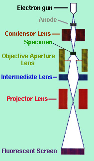
The transmission electron microscope (TEM) forms an image be accelerating a beam of electrons that pass through the specimen. These electrons are scattered at different angles depending on the density of the atom it encounters. An electron can either be "(a) undeflected, (b) deflected but losses no energy (elastically deflected), or (c) loses a significant amount of energy and is probably deflected (inelastically scattered)" (Chescoe and Goodhew, 1990). The different scattered angles produce a contrasting image because all angle scattered more than 0.5 degrees are stopped by an objective aperture (see Figure 1) situated below the specimen.
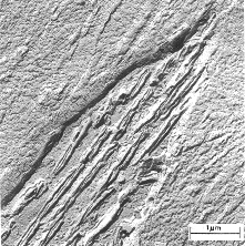
"The brightness of the image of each region will be proportional to the number of unscatttered electrons which pass through the aperture, so regions (a), (b), and (c) will appear to have a brightness ratio 91:83:4" (Chescoe and Goodhew, 1990). Therefore, light atoms, such as carbon, will appear light while heavier atoms like iron, will appear darker. The image is projected on a fluorescent screen where phases, fractures and other properties that are 2 to 3 angstroms across, can be seen. Figure 2 shows the structure of bainite which consists of ferrite and cementite phases.
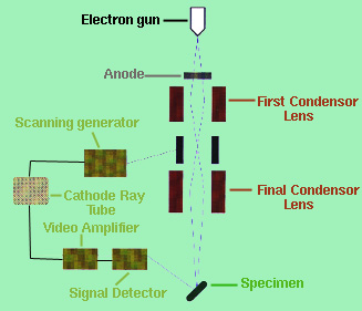
Both the optical microscope and the TEM gave the observer an internal representation of the specimen which is extremely helpful but gave little information on the objects actual appearance. In the 1960's, the SEM was built and incorporated a fine beam of electron about 200 angstroms across to scan the specimen much like the "single spot of light [that] sweeps across the face of a television screen to build an entire picture" (Gilmore, 1972). The interactions with the electron beam and the "specimen surface causes several types of energetic emissions, including backscattered electrons, secondary electrons, Auger electrons (a special form of secondary electrons), continuous x-rays, and characteristics x-rays" (Reed-Hill and Abbaschiam, 1994). The image displayed on the cathode ray tube comes from the secondary and backscattered electrons. The secondary electrons are the excited electrons emitted from the specimen by being bombarded by the electron beam. A simple schematic diagram of the SEM can be seen in Figure 3.
Phases within a material are distinguishes by the backscattering electrons. The backscattered electrons are affected by the atomic number of the atom in a way that causes the electrons scattered by the atom with the lowest atomic number to not reach the detector. These electrons will therefore appear dark in the image. As the atomic number increases, the corresponding region will appear lighter. A comparison of the images produced from secondary electrons (A) and backscattered electron (B) is seen in Figure 4. This SEM photograph shows the three different phases in a sample of niobium-silica alloy.
 (A)
(A)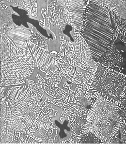 (B)
(B)
http://www.eng.vt.edu/eng/materials/classes/MSE2094_NoteBook/
96ClassProj/experimental/electron.html